A Basic Z80 System
 Some parts of this page/site are currently incomplete & will be updated asap
Other parts will change continually so use “Refresh” in your browser !!
There is extensive use of “Tooltips” text to support learning which do not seem to render on a Smartphone. This site is best viewed via a computer’s HD monitor
Basic Z80 System 1

(0) - The Z80 CPU
This is the Master 2 Device which controls all the other devices which are Slave Devices
In order to behave correctly, the Z80 needs 3 things - (1) it goes without saying that it needs a good, clean and well-regulated +5 Volt power supply, and the other two requirements are:
(1) - Generating a Clock
This is actually quite difficult and we all have our favourite circuits…
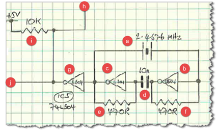
This is mine (from 1985) - tried and tested over many years. Any CPU clock circuit must be (1) very stable; (2) be 100% reliable starting up; and (3) output a clean 50/50 square wave; and (4) if you using a digital logic gate in a part analogue mode (as I am here) it must work with different manufacturers parts

It uses 3 gates (out of 6) from a 74LS04 Hex Inverter It uses a 2.4576 MHz 3 Quartz Crystal (a) as the feedback element between two digital logic gates (b) & (c) which are being “forced” to act as analogue amplifiers by 470 ohm Resistors (e) & (f) and coupled by 10nF Ceramic Capacitor (d)
The output from this arrangement is taken to the input of logic gate (g) which is being used as a digital inverter/buffer The output of (g) is taken via (j) to the baud-rate generator circuit and to Z80 pin 6 /CLK via (h)… Because /CLK is “active-low”, 10k Resistor (i) is used as a “pullup” 4
(2) - Resetting the Z80
This is much easier than generating a CPU Clock and the arrangement I have detailed below has always worked for me !!
This is a classic RC Circuit and has an RC Time-constant 5

Z80 Pin 26, /RESET at (a) is connected between a 10k ohm Resistor (b) and a 22uF Tantalum Capacitor (c)
Before applying any power, the capacitor is discharged, so therefore the positive end of the capacitor at point (a) is at 0 volts (“0v”). The negative side of the capacitor is connected to 0v
Upon applying power, and as soon as +5v appears, the 10k ohm Resistor (b) starts to charge the 22uF Tantalum Capacitor at (c) so the voltage at point (a) starts to rise towards +5v
As Z80 Pin 26, /RESET is an active-low input, the initial low voltage on (a) holds the Z80 in a RESETing state for a while
As the voltage at point (a) continues to rise towards +5v, at some stage the Z80 regards /RESET as being non-active and the the Z80 exits its internal Reset State
(3) - The Address Bus
(4) - Read Only Memory
(4)(a)
(5) - The Data Bus
(6) - The Memory Strobe
(7) - The I/O Strobe
(8) - The Read Strobe
(9) - A Parallel I/O Port Device
(9)(a)
(9)(a)
Page Source: The Zilog Z80 CPU User Manual
What the Z80 pins do…
What the Z80 Registers do…
And a truly dreadful diagram from the Zilog Z80 User Manual. It does not even show any RAM !! Then as an obvious after thought a diagram about RAM follows. All this serves to do is confuse an otherwise competant and knowledgeable engineer/hobbyist who is seeking to learn… Been there… Done that !! ↩
2.4567 MHz is a magic number as it can be divided-down and used as the baud-rate clock that a serial port needs ↩
Good circuit design calls for any “active-low” inputs (that are not tri-state) to be connected to a logic high (in this case +5v) via a “pullup” resistor ↩
With the values used the time-constant is way less than 1 second ↩